


Optical characteristic parameter measurement instruments, such as Spectrometer, Radiometer/Photometer, Laser power meter, Laser energy meter, pulse width detector, Beam quality analyzer/ Beam profiler, Polarization High-Speed Camera, etc.
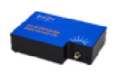
Brolight- Compact Spectrometers and Optical Power meter
Brolight provides compact spectrometers with wavelengths ranging from 180nm to 1700nm, as well as photodiode/thermopile type optical power meters.
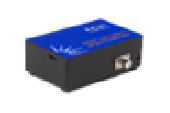
EOC- Coherent- Photodetectors for pulse-width measurement
EOC’s photodetectors are used in laboratories around the world for pulse-width measurement and pulse profiling applications, such as monitoring the output of pulsed lasers, mode-locked lasers and externally modulated CW lasers
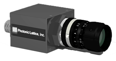
Photonic Lattice- Polarizing Optical Components & Polarization High-Speed Camera
We are not limited to providing polarization optical elements, we also provide unique products base on components, such as our proprietary birefringence measurement system, polarization high-speed camera, ultra high-speed and high-sensitivity thermal imaging camera, and carbon dioxide imaging system.
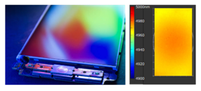
Dataray- Beam Profilers
DataRay is the leading manufacturer of ISO compliant laser beam profilers.
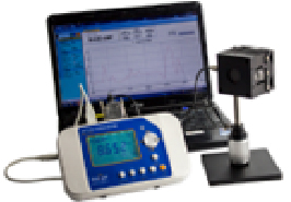
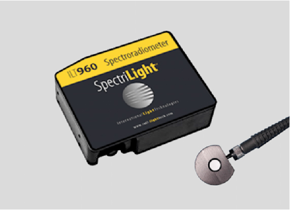
International Light- Light Meters / Radiometers/Spectrophotometers/ Spectro-Radiometers
We offer an array of light measurement products and devices including light meters, radiometers, spectrophotometers, and spectro-radiometers, for applications from ultra violet, to visible light, and infrared measurements.
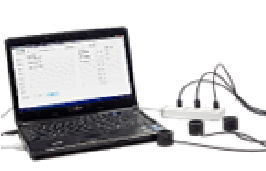
HAAS- High power Laser beam Analyzer
The Haas Laser Technologies Laser beam Analyzer System is modular design. The system includes Software, Cameras, Beam Reduction Optics, Attenuation modules and filters which enable “real-time” laer beam diagnostics from low to high power CW and pulsed lasers.
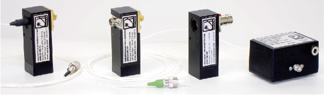
ALPHALAS GmbH – Ultrafast Photodetectors
ALPHALAS GmbH is a German laser manufacturer. As a high-tech laser company we are offering a wide range of products in the fields of lasers, optics and laser-related electronics.

Brolight was founded in 2012, Hangzhou, China.
Brolight is a professional manufacturer of Science Education Apparatus & Photonics Instrument. We manufacture various experimental teaching and training kits for physics and optoelectronics, and light analysis solutions base on Spectrum & intensity,to bring customers the high-quality, affordable, and reliable products.
The optical analysis products include spectrometers and optical powermeters:
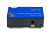
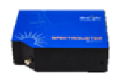
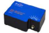
Spectrometer products:
| Description | Ref. Photo | Series | Wavelength Range(nm) |
Resolution FWHM (nm) |
Remark |
|
VIS-NIR Compact Spectrometer |
 |
BIM-6001A | 315~1100 | 1~0.35 | |
| BIM-6002A | 180~1100 | ||||
|
VIS-NIR High Resolution Spectrometer |
 |
BIM-6601A | 315~1100 | 0.35~0.08 | |
| BIM-6602A | 180~1100 | 0.35~0.1 | |||
| BIM-6606 | 200~1100 | 0.35~0.06 | |||
|
UV-NIR High Sensitivity Spectrometer |
 |
BIM-6703 | 200~1100 | 1~0.35 | The high sensitivity on the range 500-900nm, Suit to Raman Application |
| BIM-6704 | The high sensitivity on the range 200-500nm, Suitable to UV Range | ||||
|
UV-NIR High Sensitivity & Resolution Spectrometer |
 |
BIM-6603 | 200~1100 | 1~0.1 | The high sensitivity on the range 500-900nm, Suit to Raman Application |
|
NIR spectrometer |
 |
BIM-6805 | 950-1700 | ~10nm | |
 |
BIM-6809 | 920-1700 | ~5nm |
Laser Power Meter Products:
| Communication | Power Meter | USB | BT | |
| Description |
The outputs data through the power meter (can be displayed directly or connected to a PC via USB) |
USB or USB Hub as communication interface, displayed on the PC |
Data transmission through BT, displayed on the mobile phones or tablets(Android Only now) |
|
|
Detector |
Si, 380~1100nm Power density:10mW/cm2 |
√ | √ | × |
|
UV-Si, 80~1100nm Power density:1mW/cm2 |
√ | √ | × | |
|
InGaAs: 800~1650nm Power density:10mW/cm2 |
√ | √ | × | |
|
Thermopile: 0.19~20µm Power density:10kW/cm2 |
√ | × | √ | |
|
Remark: |
Photodiode detector, can be configured with an integrating sphere. | |||
![]()
Photonic Lattice founded in Sendai, Japan in 2002.
It’s core technology is photonic crystal technology, in which micro-polarizer arrays with various axis directions are freely patterned and stacked on a single wafer using sputtering technology. This technology is used as a core component in optical communications (polarization multiplexing), semiconductors (inspection using DUV light), precision processing (beam shaping), and other cutting-edge equipment in various fields.
Today, through research and development of applied technologies such as special optics and computational algorithms, we have realized unique products such as our proprietary birefringence measurement system, polarization high-speed camera, ultra high-speed and high-sensitivity thermal imaging camera, and carbon dioxide imaging system, enabling us to visualize and measure phenomena that were previously difficult.
PRODUCT:
We provide optical elements, optical modules, inspection devices, custom development, and contract testing services using our unique optical technologies.
- ● Photonic Crystal Polarizing Optical Components
- ● 2D Birefringence Measurement System
- ● In-line/off-line mapping-type birefringence measurement system
- ● High-speed infrared camera / Infrared Measurement Equipment
- ● High-speed Polarization Camera
- ● Polarization Imaging Camera
- ● Ellipsometric measurement
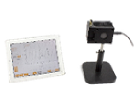
2D Birefringence Measurement System
PA/WPA series systems provide high-speed birefringence measurement of transparent materials, such as transparent parts for residual stress evaluation, or transparent films for the evaluation of phase uniformity. Ranging from microscopic to macroscopic (~50cm), the field of view adapts to any measurement situation, and there is a system for each size.
- ● PA series measures birefringence and phase difference with a high resolution of 5 million pixels at high speed, for low phase difference with a measurement range of 0 to 130 nm. Suitable for measurement of glassware and other low phase difference targets.
- ● WPA series expands the measurement range of phase difference from 0 to 3,500 nm by measuring birefringence/phase difference distribution over three waves. Suitable for measuring large transparent resin products.
PA/WPA-NIR series
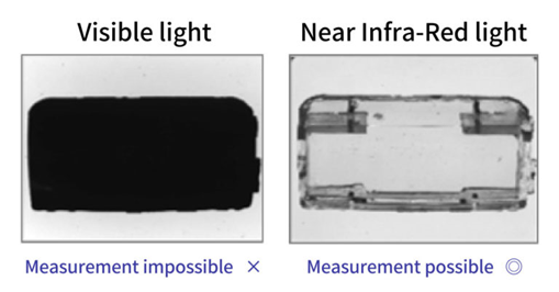
Operating at 850nm wavelength, this system provides strong tools for process and quality control of pieces not transparent at visible wavelengths, such as special resins and chacolgenide, used for example in LIDAR and face recognition systems.
In-line/off-line mapping-type birefringence measurement system
With KAMAKIRI, the entire film surface is inspected. Therefore, even if a sudden optical irregularity occurs, an alarm can be generated real-time, to prevent any defective area outflow.
From “Visualization” to “Automated Inspection”Prevention of outflow of defective products & quick detection of defects
- ● As displays become higher in resolution and contrast, and as manufactures improve image quality, a high degree of phase shift and principal axis orientation uniformity within the film plane is being pursued.
- ● Furthermore, from an environmental perspective, it has become important to designate production lots to be disposed of and film trimming areas.
- ● By using KAMAKIRI, which combines a unique polarization high-speed camera and scanning system, it is now possible to inspect and record birefringence in the film plane with high accuracy in an extremely short time, both on the production line and in the research lab.
Numerous installation results
- ● Since its launch at the end of 2014, more than 50 KAMAKIRI series products have been installed by optical film manufacturers and glass/lens molding manufacturers in Japan, Korea, and China.
- ● Especially for optical film manufacturers, there are many different types of production lines, each with different requirements.
- ● By confirming the status of customer’s production line, we can propose the optimal system configuration.
- ● We have manufactured and installed small systems for 200mm width measurement and large systems exceeding 5m width.
High-speed infrared camera / Infrared Measurement Equipment

We propose an infrared R&D measurement system based on the world’s highest class high-speed and high-sensitivity infrared camera technology. It is suitable for various new applications such as high-speed temperature measurement, CO2 gas visualization, or welding temperature analysis.
Visualization of momentary temperature changes
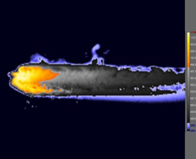
- ● With our cooled infrared high-speed camera, thermal noise is reduced to the utmost limit by cooling the image sensor to -190°C, enabling high-precision, high-speed thermal imaging measurements, that have been difficult to achieve in the past.
- ● This makes it possible to accurately measure high-speed phenomena, such as the temperature rise at the moment of breakage in a tensile test, the temperature rise of a workpiece during laser processing, or the temperature measurement of a high-speed moving object. Also, by detecting extremely small temperature changes with high precision, it is possible to evaluate, for example, the temperature rise of a semiconductor chip during operation or temperature irregularities in a liquid during temperature rise.
Visualization of CO2 gas
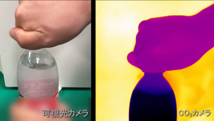
- ● By visualizing invisible gases such as CO2, methane, ethane, ethanol, toluene, etc., one could detect and quantify leakages from pipes, exhalation flow, or characterize bare air flow using CO2; gas as an inexpensive tracer.
- ● A particular concern when visualizing CO2 is that it is generally difficult to distinguish from water vapor.
- ● On the other hand, CO2 cameras can discriminate gases by spectrally filtering infrared absorption at specific wavelengths.
- ● In the 4.3 micron wavelength band, CO2 is much more absorptive than water vapor, so this concern can be overcome.
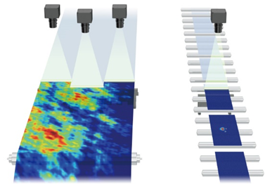
High-speed Polarization Camera
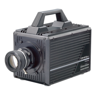
CRYSTA, the world’s fastest high-speed polarization camera, can visualize internal stress and orientation structure of transparent materials real-time. It is of great help in various R&D fields, such as biotechnology, defense or aerospace technology.
- ● Visualization of internal stress distribution during material processing and analysis of processing conditions
- ● Evaluation of stress propagation around cracks in impact test/fractures
- ● Dynamic observation of crystal axis and orientation state for liquid crystal/crystalline materials
- ● Visualization of flow stress distribution generated by viscoelasticity and soft matter
Polarization can measure and visualize various physical quantities and physical properties.
- ● Polarization is “light that vibrates in regular direction” and it cannot be recognized by human eyes. Since the polarization state varies depending on the internal structure of the transmitted object and the surface shape of the reflected object, it is recognized that it can be applied to the measurement of various physical quantities and the visualization of phenomena by measuring the polarization state of the incident light and the transmitted light to/from the object.
- ● Furthermore, the combination of “Polarization” and “High-speed imaging” technology will enable new image analyses that were previously unimaginable, such as examining the load applied to tools during the processing of transparent materials from images, visualizing stress propagation and relaxation processes in impact tests and flow phenomena, and quantitatively measuring the spatial performance uniformity of alignment films in a non-contact manner.
Polarization Imaging Camera
PI/WPI cameras are capable to obtain polarization information real-time, as a normal image, and at high-resolution.
They are used in many areas including recognition of dark objects using their polarization signature, real-time polarization monitoring of laser beams, etc.
In addition to PI capabilities of recording the Degree of Linear Polarization (DOLP) and main axis orientation angle, WPI provides full-fledged recording of the Stokes parameters and Degree of Polarization (DOP), which is necessary in partial polarization situations.
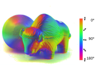
Observation of surface bumps,made clear by polarization effects
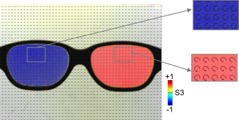
Polarization allows detecting small edges and surface irregularities that would be difficult to see using normal cameras. Polarization imaging especially shines when observing dark objects.
 |
 |
|
| Normal image |
Polarization image Surface bumps are distinctly seen on polarization images. |
Evaluation of new materials (carbon fiber …)
Using reflected light, polarization can be used to observe and quantify in real-time the orientation of the fibers in a CFRP (Carbon Fiber Reinforced Polymer) sample.
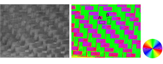
Evaluation of new materials
Full-Polarization imaging with WPI
Full-Polarization imaging with WPIPolarization cameras on the market, including PI, provide only limited polarization information, not the whole picture.
In contrast to such cameras, WPI systems have access to the full-fledged Stokes parameters, allowing discernment among right-handed, left-handed, elliptical and circular polarization states. Furthermore, WPI systems differentiate between polarized and unpolarized light, and do not mix up elliptical polarizations with unpolarized light. The WPI system is the optimal choice for full polarization measurement.
The blue part is right-handed circular polarization (RCP), the red part is left-handed circular polarization (LCP)
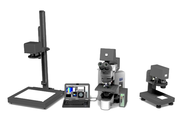
Ellipsometric measurement
Those systems measures the thickness and refractive index of ultra-thin films. They realizes high-speed measurement for complete 2-D distribution featuring zooming to micro-scale areas. They are used mainly for semiconductor wafers and display panels evaluation.
High-speed, non-destructive, high-accuracy measurement of thin film thickness & refractive index at high resolution is now possible.
We support quality management and process control with unprecedented data volume and software functionalities adaptable to your needs.
High-speed
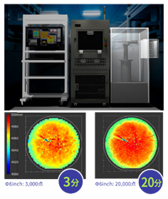
High-speed evaluation of full area wafers (up to 12 inch).
Using an unprecedented amount of data, you can provide feedback to your troubleshooting process and bring your quality control to a new level.
- ● Thickness measurement upgraded from “point” to full-fledged “surface” evaluation
- ● Whole surface evaluation provides great insights for process evaluation
High-resolution【ME-210(-T)】
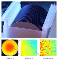
In addition to its large surface measurement capabilities of wafers up to 12 inches, the ME-210(-T) provides a high-resolution mode, allowing zooming into areas as small as a few micrometers.
Measurement area size: up to 12 inches (standard: 8 inches)
Spot size:
- Standard mode : 0.55 mm
- Intermediate mode: 55μm
- High-resolution mode: 5.5μm
Thin film of transparent substrate measurements available
With ME-210-T, we made possible the evaluation of objects that are usually too difficult to evaluate using standard ellipsometric techniques, such as organic thin films for OLED, etc.
Simple & compact【SE-101】
This compact point measurement system provides high-accuracy and high-repeatability thin film measurements.
Its detachable head can be used as a separate module to integrate into your manufacturing infrastructure.
![]()
![]()
DataRay Inc. was founded in 1988, CA,USA.
DataRay is the leading manufacturer of ISO compliant laser beam profilers. We manufacture a variety of laser beam profiling solutions to bring the photonics industry high-quality, affordable, and reliable products. Our solutions include laser beam profiling cameras, scanning slit beam profilers, M² measurement systems, and specialized beam profiler systems. We offer solutions for a wide variety of applications and wavelengths. Our beam profiling systems are designed and manufactured in the USA and come with an industry-leading 3-year warranty.
We were the first to market with:
- ● Beam profiling software for Windows
- ● Windows 95 compatible CCD beam profiling cameras
- ● Software control of CCD electronic shutter
- ● Micron capable, linear scan, dual-mode Slit/Knife Edge beam profilers which fully meets the ISO 11146 standard for beam profiling instruments
- ● Compact multi-plane scan heads for focused beams, collimation and M² measurement
- ● 14-bit ADC digital Megapixel CCD beam profiling cameras
- ● USB 2.0 port-powered beam profiling cameras
- ● Windows 7 support
THE DATARAY Advantage:
|
Broad applications Products featuring:
|
 |
Wide bandwidth DataRay's product portfolio covers wavelengths from deep UV to FIR |
 |
No hidden costs of ownership All DataRay systems include a 3-year warranty; any necessary servicing within this period is at no charge, including parts and labor (excluding damage by customer) |
 |
ISO 11146 compliant beam profiling We use XY plane scanning slit motions which strictly comply with the Standard's requirement for a slit or knife-edge scan to be made in a plane perpendicular to the propagation axis |
 |
Free, user-friendly software We provide versatile software with free downloadable updates for the life of your product |
 |
Localization support You always can find a local professional distributor near you. In China, Pls contact A&P. |
Product Series:
1.Beam Profiling Cameras

DataRay manufactures three series of beam profiling cameras: WinCamD, BladeCam, and TaperCamD cameras. These CMOS and VO microbolometer-based cameras cover a broad range of different wavelengths from 190 nm to 16 μm.
2.Scanning Slit Beam Profilers (Si, Ge, and InGaAs detectors)
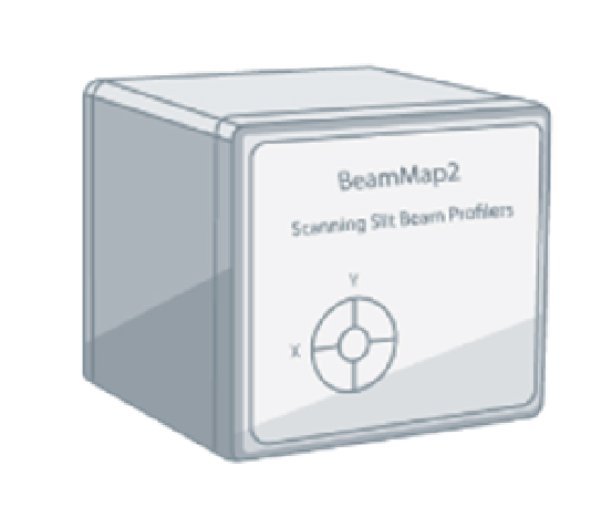
DataRay manufactures two types of scanning slit beam profilers: the patented BeamMap series, which offers real-time M², divergence, focus and alignment management, and the Beam’R series which provides affordable, compact, and precise beam profiling. All of our scanning slit beam profilers are available with Si, Ge, and InGaAs detectors, covering wavelengths from 190 nm to 2500 nm.
3.Specialized Beam Profiler Systems (Inspired by customers)
In addition to beam profiling cameras and scanning slit beam profilers, DataRay offers specialized beam profiler systems. These systems offer solutions for complex applications. The large beam profiling system is suitable for beams up to 200 mm image area, and the line laser profiling system provides for direct measurement of line lasers up to 200 mm in length.
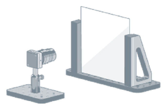
4.Accessories
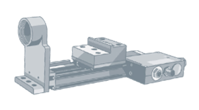
DataRay offers various beam profiler accessories covering beam attenuation, optics, translation stages, UV and IR converters, and more.
![]()
![]()
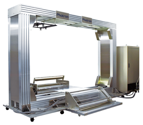
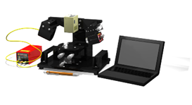
HAAS Laser Technology Inc.
Haas Laser Technologies, Inc. is a leading innovator in custom laser beam delivery components. Founded by Gilbert Haas in 1992, our mission is to set industry standards for innovation, reliability, and quality. With a 35,000+ square foot facility in Flanders, New Jersey, we offer a vast selection of laser beam delivery components globally. Our vertically integrated team includes experienced engineers, advanced manufacturing, and a state-of-the-art machine shop.
Far East and European distributorships have demonstrated Haas Laser Technologies' commitment to provide and support its products worldwide. It is no wonder that Haas Laser Technologies has emerged as one of the top recognized world leaders in laser beam delivery systems.
Haas currently has thousands of its products in continuous operation 24 hours a day, 7 days a week at installations through out the world at companies such as Chrysler, General Motors, Ford, General Electric, Air France, and Hewlett Packard.
The main products include:
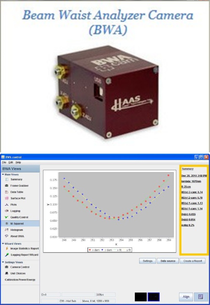 |
● Laser Beam Diagnostics In every laser application, the laser beam profile provides valuable information for the most efficient use of the laser. By monitoring the laser beams spatial profile, circularity, centroid, astigmatism and M2 values, you have early warning of any problems with the laser and entire beam delivery optical system. This relates to increased quality, process reliability, and reduced scrap. The Haas Laser Technologies Laser beam Analyzer System is modular design. The system includes Software, Cameras, Beam Reduction Optics, Attenuation modules and filters which enable “real-time” laer beam diagnostics from low to high power CW and pulsed lasers. The design provides both near-field and far-field instantaneous laser beam measurement, analysis and monitoring with “no moving components”. The BA-CAM and BWA-CAM software is designed based on ISO 11146 and ISO 13694 international standards. Full image based second moment techniques, knife edge and equation fitting (Gaussian, Super Gaussian, and Super Donut) techniques are used to determine quick and reliable standard beam parameters. Calculated results can be viewed in tabular form as well as logged to view changes over time. Visualization windows include X and Y axis plots, 3D view of laser beam, histograms and database reports. |
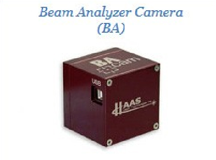 |
BA-CAM The Beam Analyzer (BA-CAM) provides “Real-Time” far-field viewing, measurement, analysis and monitoring of laser spatial distribution, laser power, beam diameter, beam ovality, beam center and beam centroid. The BA-CAM can also monitor the laser beam for degradation, stability, power, alignment and tuning. |
 |
BWA-CAM The Beam Waist Analyzer (BWA-CAM) provides “Real-Time” near-field M2 measurements with no moving components. The (BWA-CAM) provides instantaneous analysis and monitoring of the laser beam and all active optical elements. |
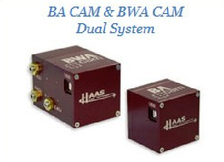 |
BA-CAM + BWA-CAM The dual systems incorporates both the Beam Analyzer (BA-CAM) and the Beam Waist Analyzer (BWA-CAM) to provide “Real-Time” near-field and far-field viewing, measurements and analysis of the laser beam. |
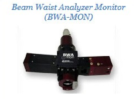 |
BWA-MON The BWA-MON is a modular focus head design configured for the Beam Analyzer (BA-CAM) and the Beam Waist Analyzer (BWA-CAM) for most applications and laser wavelengths. The design contains no “moving components” and provides instantaneous measurement and analysis of the laser beam and its optical elements. |
![]()
![]()
About International Light
For over fifty years International Light has been developing products and solutions that meet a broad range of needs and solve a variety of challenges. ILT combines technical lighting and light measurement expertise to provide products and services that shine.
International Light Technologies was formed when Gilway Technical Lamp merged with International Light. Gilway and International Light have long and proud reputations for delivering exemplary customer service, on-time delivery, and technical expertise. Formed in 1969, Gilway Technical Lamp has provided customers with off-the-shelf and customized solutions for a full spectrum of light sources. Since 1965 International Light has been solving the inherent difficulties in light measurement through the design and manufacture of a wide range of light measuring instruments, including the most accurate light meters on the market.
In February of 2022, ILT was acquired by Ocean Insight. International Light Technologies offices, R&D efforts, certified state-of-the-art testing and calibration lab, warehousing and much of its manufacturing are located in Peabody Massachusetts, just 15 miles north of Boston.
Why International Light
Why should you partner with ILT to overcome your latest challenge? Innovating and problem-solving are what we do. We have over a half-century of experience working with companies of all shapes and sizes, and across a broad range of industries, to deliver products and solutions that tackle the toughest obstacles. ILT employs a team of highly skilled experts in the areas of electrical, optical, mechanical, quality and manufacturing engineering. Our staff will work with you to ensure you get a solution – whether off-the-shelf or tailor-made – that is right for you. In today’s tumultuous environment where the big guys are struggling to keep up and many entrants come and go, ILT is continuing to deliver products and solutions that solve problems, are designed and manufactured to the highest quality standards, and can be brought to market quickly and cost effectively.
What We Offer
ILT has been developing solutions for lighting and light measurement for more than 50 years. We have an extensive catalog of off-the-shelf options, but the real benefit we bring to our customers is our ability to develop customized solutions that meet your specific requirements.
We offer an array of light measurement products and devices including light meters, radiometers, spectrophotometers, and spectro-radiometers, for applications from ultra violet, to visible light, and infrared measurements. We also offer supporting accessories including, detectors, filters, input optics, integrating spheres and calibrations.We engineer our products to withstand the many harsh applications required from underwater applications to direct exposure to high levels of UV, to last years of use.

Our Commitment to Our Customers
At ILT we are committed to providing our customers with the highest quality products, prompt and courteous customer service, and world-class technical support. We realize that much of what we make ends up as part of a solution for our customers’ customers. When you partner with ILT you can be confident that we will stand by our products and work through any issues to resolution.
Our Commitment to Quality
ILT is committed to delivering the highest quality products and services to our customers. Our employees use the latest tools to ensure all of our products are designed and manufactured to meet our stringent requirements for durability, reliability, efficacy and cost efficiency.
To ensure that this commitment is understood, implemented and maintained, all of our employees are familiar with our policy and understand their requirements within the Quality System through training and access to our Quality Manual. We are an ISO9001:2015 certified organization for quality management, and all of our products are backed by a warranty. ILT is also ISO13485:2016 certified.
ILT is an ISO/IEC 17025:2017 Accredited lab. This certification allows us to calibrate ILT-branded and non-ILT branded light meters and spectroradiometers. Visit our Calibrations page here to see all of our calibration services.
![]()

ALPHALAS GmbH – Ultrafast Photodetectors
ALPHALAS GmbH is a German laser manufacturer. As a high-tech laser company we are offering a wide range of products in the fields of lasers, optics and laser-related electronics.
The main activities of ALPHALAS include development, production and sales of lasers, laser systems, laser-related electronics and components. The main products are advanced modelocked, CW and Q-switched diode-pumped solid-state lasers. ALPHALAS is specialized in short pulses (subnanosecond, picosecond and femtosecond) and microchip design but we are offering practically all common types of DPSS lasers featuring high efficiency and compact design.
A variety of optoelectronic devices and components aimed at measurement of various laser parameters is available. We have a large selection of optical and laser components, polarization optics, laser and nonlinear crystals as well as exotic and unconventional components. Most components are available from stock.
The UPD series of ultrafast photo detectors are best suited for mea surement of optical waveforms from DC to 25 GHz. Various models feature rise times as short as 15 ps and cover the spectral range from 170 to 2600 nm
![]()